
Researchers
- Péter Németh (PhD)
- István Fórizs (PhD)
Institute engineer
- Máté Szabó
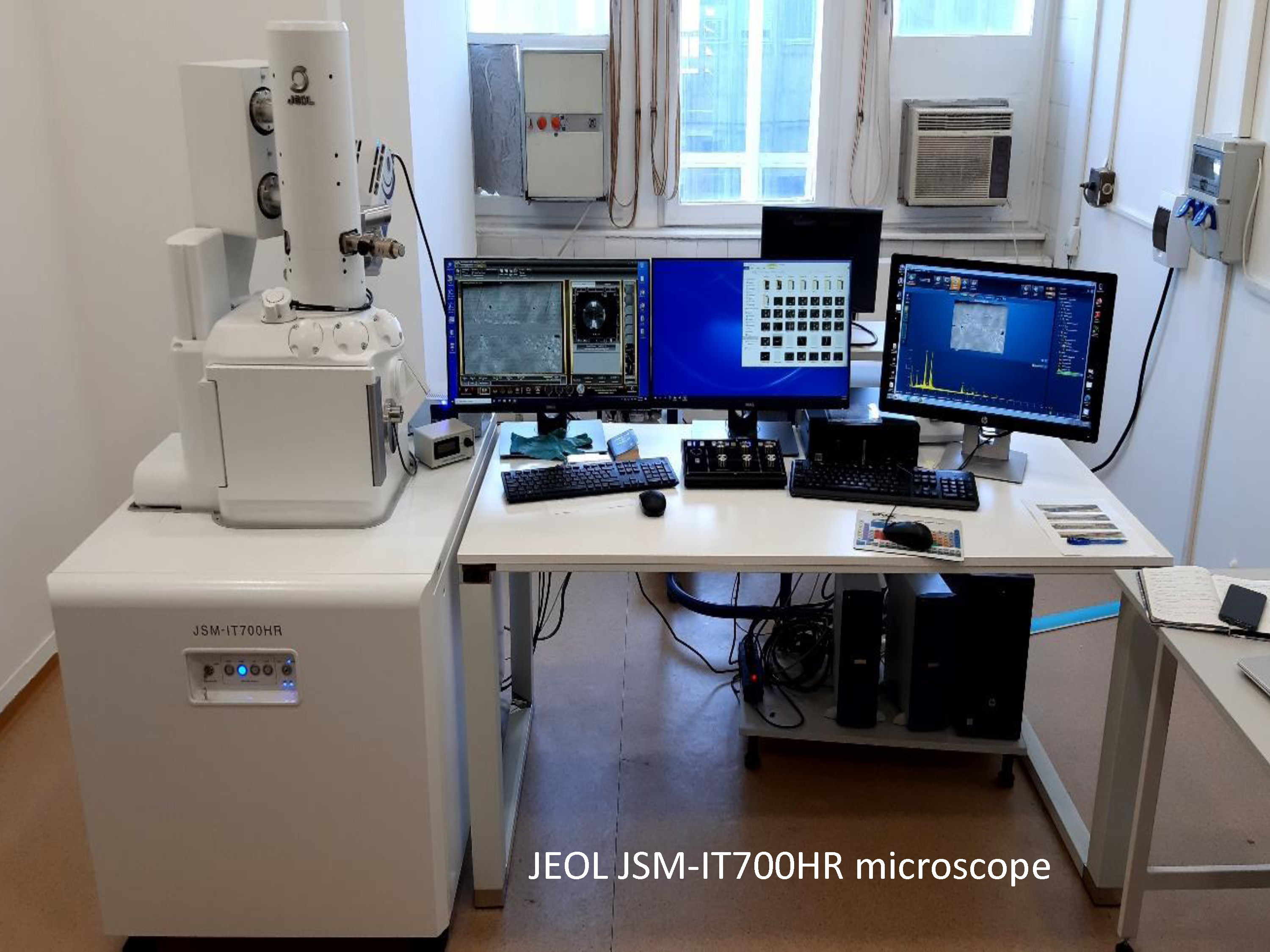
The scanning electron microscope laboratory in the Institute for Geological and Geochemical Research was established thanks to a successful ELRN infrastructure grant. The financial support made it possible to replace the more than 40 years old JEOL JCXA-733 electron microprobe with a modern, field-emission gun-equipped JEOL JSM-IT700HR microscope. The new instrument has significantly expanded the material investigation possibilities of the mineralogical, geochemical, geological, and archaeometric researches carried out at the institute. The field emission source allows the device to achieve a spatial resolution of up to 1 nanometer, i.e., the morphology and texture of the sample can be investigated with great detail. The low accelerating voltage (1 keV) setting ensures the in-depth examination of surface structures and nanoparticles. Thanks to the low-vacuum and low-acceleration voltage modes, insulating materials can also be studied without more serious sample preparation (without carbon coating). The latter - preserving the original condition - is especially important for archaeological materials and cultural heritage objects.
Scope of activities
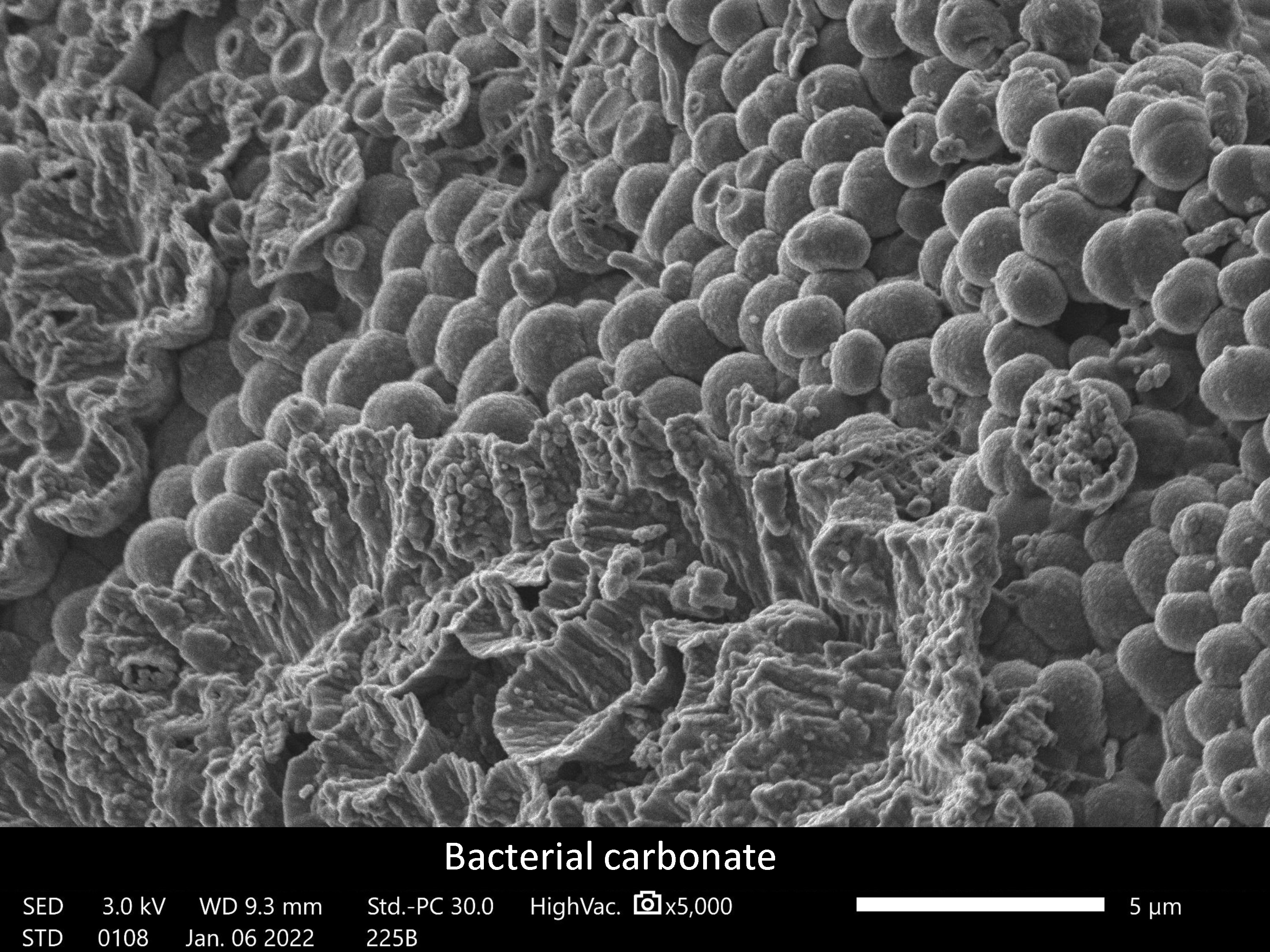
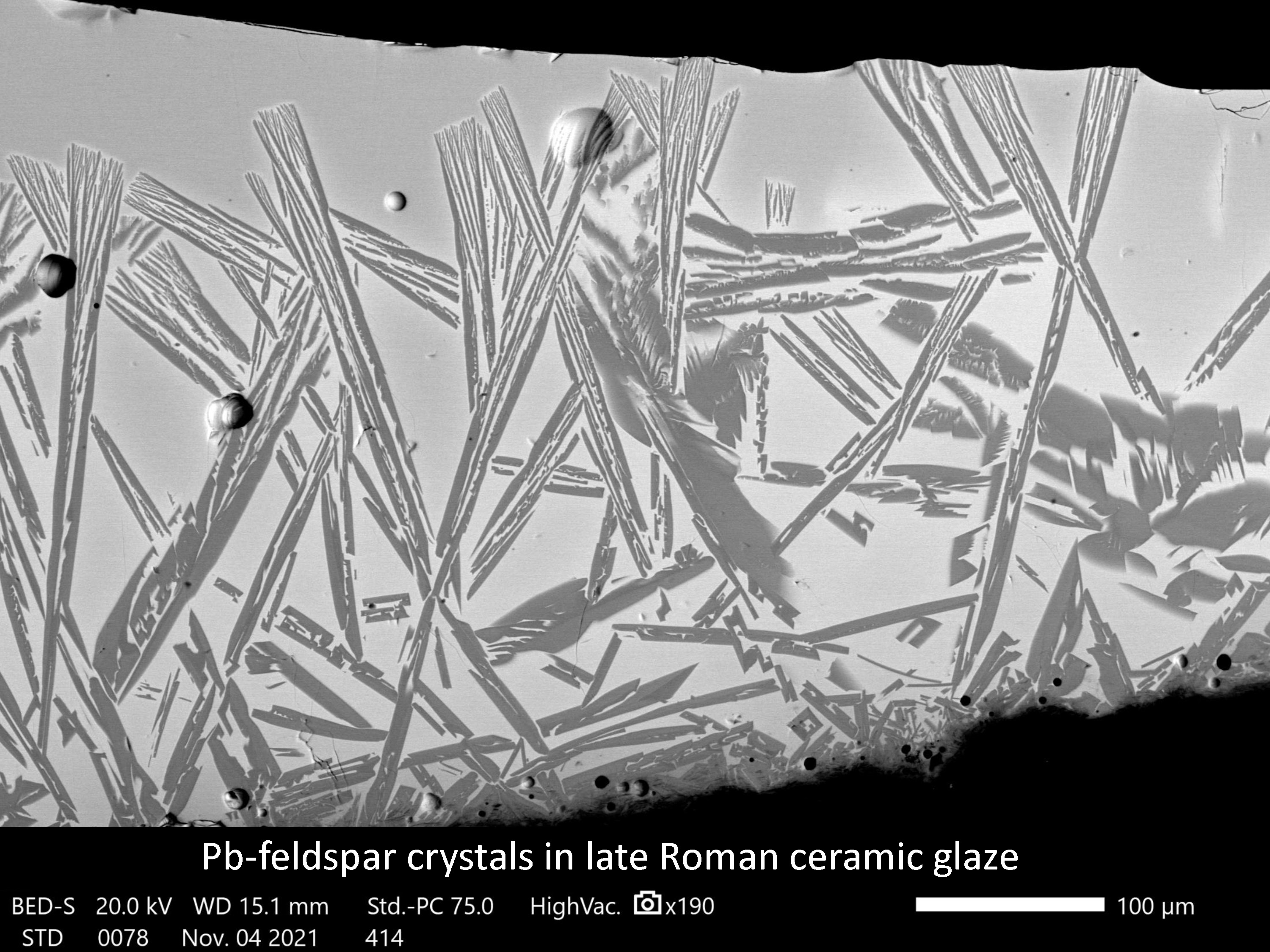
The instruments and the sample preparation equipment enable state-of-the-art material characterization of minerals, rocks, ceramics, metals, other inorganic and organic samples. They provide morphological and chemical composition information for the substances to be tested. The main profile of the laboratory is the examination of geological samples, but it has significant experience in the analysis of (industrial) ceramics, metals, glass and other cultural heritage materials. In the field of biology and related sciences, the instruments allow the submicron characterization of plants, insects, bacteria and other microscopic organisms, among others.
Instruments and available methods
1. JEOL JSM-IT700HR scanning electron microscope (SEM)
Morphological images with a spatial resolution of 1.0 nanometer can be taken at the highest magnification of the microscope. There are several ways to eliminate sample charging: low-acceleration imaging, CF-Charge Free Scan mode, and a self-pumping low-vacuum mode. The unique feature of the robust sample table is eucentricity throughout the entire X, Y, Z working range. The settings of the observation point are retained even if the sample table is moved or tilted, the observation point remains in place during the movement. With the attached JEOL energy dispersive spectrometer, chemical elemental analysis and elemental mapping from boron can be performed with a spatial resolution of ~10 microns.
2. SMZ800N NIKON stereomicroscope
Samples can be examined simultaneously with the microscope in the magnification range of 1.0x to 6.3x and that of 10x to 63x thanks to the Achro objective. Images are captured with a Truechrome 4K PRO digital camera.
3. JEOL JFC-1200 Fine Coater and JEOL JEC-530 Auto Carbon Coater
Insulating materials can be made conductive with these devices.
4. Image processing and quality analysis
During SEM studies, images are taken that contain morphological, topographic, and chemical composition information specific to the test material. Additional image details can be obtained during image processing. Among other things, we can determine the exact composition of the sample, the size and distribution of the particles, and get closer to learning about the phases that make up the sample.